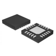
CA51F003N2
The CA51F003N2 chip is an 8-bit microcontroller based on the 1T 8051 core. Under normal circumstances, it runs 10 times faster than the traditional 8051 chip and has superior performance. Built-in 18K Flash program memory can be repeatedly programmed, and built-in 1K SRAM brings great convenience to users. It not only retains the basic characteristics of the traditional 8051 chip, but also integrates functional modules such as 12-bit ADC, 16-bit PWM, UART, IC, operational amplifier and low voltage detection (LVD), and supports online simulation function. Support three power saving modes: IDLE, STOP and low-speed operation to adapt to applications with different power consumption requirements. Widely used in consumer electronics and home appliances.

Product Details
core
CPU: 1T8051, which is 10 times faster than the traditional 8051.
Compatible with 8051 instruction set and dual DPTR working mode.
storage
Flash: 18K bytes, supporting repeated erasing.
Flash can be divided into program space and data space. The data space can be used to store data that needs to be saved when power is off, and EEPROM can be omitted.
RAM:256 bytes of internal RAM and 1024 bytes of external ram.
operating voltage
Working voltage: 1.8-5.5V
Clock system
Built-in low-speed RC oscillator: 131KHz
Built-in high-speed RC oscillator: 32MHz, with an accuracy of 1% (3.3v @ 25℃) (when used as the system clock, it is divided by 2 by default, that is, 16MHz).
External high-speed oscillator: 1-24MHz
External clock input: 1-24MHz
TMC function
The clock source is a built-in low-speed RC oscillator, and the minimum interruption time is 512 clock cycles of the low-speed RC oscillator.
The configurable interruption time is 1-256 minimum unit times.
Interrupt system
15 active interrupt sources
Two-level interrupt priority supports interrupt nesting.
10 external interrupt sources, and each external interrupt can be configured with any signal pin as an interrupt input pin.
timer
Three 16-bit universal timers: Timer 0, Timer 1 and Timer 2.
General purpose input/output port (GPIO)
Supports up to 18 GPIO ports, and supports push-pull, open-drain, strong pull-up, weak pull-up, strong pull-down, weak pull-down and high resistance modes.
Analog/digital converter (ADC)
Support 12-channel 12-bit SAR ADC with built-in operational amplifier and comparison function.
Supports three reference sources: VDD, internal reference and external reference.
The VDD voltage can be measured when the internal voltage is selected as the reference voltage.
Supports the configurable comparator mode.
Support the detection signal to be converted after being reduced by the operational amplifier, and the reduction ratio can be selected.
ADC can directly detect the output of op amp a.
ADC can be used in combination with PWM, and the ADC conversion is started by PWM interrupt.
Operational AMPlifier (AMP)
Operational amplifier A has a built-in correction mechanism, and the offset voltage is less than 0.5mV at full temperature after correction.
PWM
Support 6-channel PWM, and the cycle and duty cycle can be configured arbitrarily within 16-bit range.
PWM[0]-PWM[5] Any GPIO pin can be selected as the PWM output pin.
It supports complementary mode and dead-time control, and can be used to drive DC brushless motor.
Supports the setting of edge alignment and center alignment modes.
Support software braking and hardware braking.
Support PWM pause function
Support the function of directly outputting internal clock.
Support PWM interrupt
Low voltage detection (LVD)
The voltage detection range can be configured, and four gears can be selected: 2.0V/2.7V/3.7V/4.4V.
Low voltage reset or interrupt can be set.
Reset mode
The chip supports a variety of reset sources: hard reset, soft reset, watchdog reset, low voltage detection reset and power-on/power-off reset.
watchdog
27-bit watchdog timer, 16-bit precision adjustment, configurable watchdog reset or interrupt.
Universal serial interface (UART1/UART2)
Supports 2 UART interfaces.
Support 1 byte receive cache
SPI interface
Built-in 1 4-wire SPI interface, supporting master-slave mode.
I2C interface
Built-in 1 I2C interface supports master-slave mode and standard/fast/high-speed mode.
buzzer
Built-in 1-way buzzer drive output
Multiplier and divider (MDU)
Support 16-bit× 16-bit multiplication in one clock cycle.
Support 8 clock cycles 32-bit ÷ 32-bit division.
Support left-right shift operation of 32-bit data in one clock cycle.
Program download and simulation
Support ISP and IAP
Support double-wire and single-wire online simulation function
low power consumption
STOP mode, current < 7uA
IDLE mode, current < 15uA
Low speed operation mode, current < 25uA
Package type: QFN20(3X3mm)
For detailed information, please call 86)18823661714 (same as WeChat).


