CA51M151S3A
The CA51M151S3A chip is an 8-bit microcontroller based on the 1T 8051 core, which not only retains the basic characteristics of traditional 8051 chips, but also runs 10 times faster than traditional 8051 chips in general, with superior performance. The chip is equipped with 8 KB MTP program memory, 256 bytes of internal RAM, 512 bytes of external RAM, and 512 bytes of EEPROM. It also integrates 14 channels of 12 bit ADC, 14 channels of Touch Key (without external capacitors), 16 bit PWM, I2C, 2 channels of UART, SPI, TMC, low voltage detection (LVD) and other functional modules. Supports PWM, I2C, UART peripherals that can be mapped to any pin. The I/O push-pull output mode has 4 levels of selectable current and 2 levels of selectable current. The software can achieve dual scan LED screen display function. It also supports three power-saving modes: IDLE, STOP, and low-speed operation to adapt to applications with different power consumption requirements. Its powerful functions and superior anti-interference performance make it widely applicable to various household appliances and consumer products.

Product Details
Kernel
CPU: 1T 8051, higher speed 10 times faster than traditional 8051
Compatible with 8051 instruction set, dual DPTR working mode
Memory
MTP program memory: 8KB, with more than 1000 repeated erasures
EEPROM: 512 Byte, used to store data that needs to be saved after power failure, with more than 100000 repeated erasures
RAM: 256 Bytes internal RAM, 512 Bytes external RAM
Working voltage
Working voltage: 2.7V~ 5.5V@Fosc =8MHz
2.2V~ 5.5V@Fosc =4MHz
Working temperature
Working temperature: -40 ℃~+85 ℃
Clock system
External low-speed oscillator: 32.768KHz
Built in low-speed RC oscillator: 128KHz
Built in high-speed RC oscillator: 8MHz, accuracy of ± 2% @ 5V/25 ℃ (factory calibrated)
Timer
Three 16 bit universal timers: Timer 0, Timer 1, Timer 2
Universal Input/Output Port (GPIO)
Supports up to 14 GPIO ports (different models may vary)
Supports push-pull, open drain, pull-up, pull-down, and high resistance modes
When outputting by push-pull, there are four levels of selectable push current for GPIO: 12mA, 10mA, 8mA, 6mA@ VDD=5V
When pushing and pulling output, there are two levels of GPIO current available: 16mA and 8mA@ VDD=5V
GPIO can be software simulated as a 1/2 BIAS LCD driver without the need for external resistors
TMC function
The clock source of TMC timer can be selected as IRCL or XOSCL
The minimum unit of interruption time is 512 IRCL clock cycles when the clock source is selected as IRCL, and 128 XOSCL clock cycles when the clock source is selected as XOSCL
The configurable interrupt time is 1-256 minimum unit times
Interrupt system
7 valid interrupt sources - two-level interrupt priority, supporting interrupt nesting
5 external interrupt sources INT0~INT4
External interrupt trigger edge selection: INT0~1 (rising edge, falling edge), INT2~4 (rising edge, falling edge, double edge)
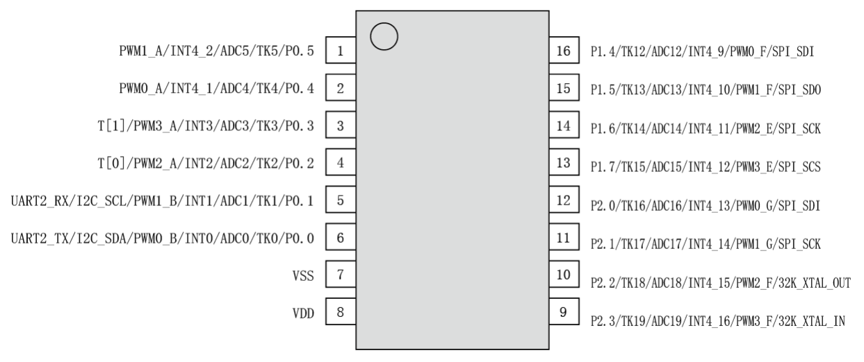
Interrupt input pin selection: INT0 (P0.0), INT1 (P0.1), INT2 (P0.2), INT3 (P0.3), INT4. Any GPIO pin except for P0.0~P0.3 can be selected as the interrupt input pin
Analog to Digital Converter (ADC)
Supports 14 channels of 12 bit SAR ADC (different models may vary)
Supports two reference voltage sources: VDD and internal reference
Selecting internal voltage as the reference can measure VDD voltage
Touch Key
Built in touch sensing controller, no need for external capacitors
Larger support for 14 touch channels (different models may have differences)
High anti-interference performance, compliant with EMC (CS dynamic 10V, EFT 4KV) standards
Support touch interruption
Supports parallel connection of touch channels, which can be used to achieve low power consumption mode
PWM
Supports 4 PWM outputs, each path can be individually controlled, and the cycle and duty cycle can be freely configured within a 16 bit range
Supports direct output of internal clock function
Support PWM interrupt function
Each PWM output pin can be mapped to different GPIO pins
Universal Serial Interface (UART1/UART2)
Supports 2 full duplex serial ports
Supports 1-byte receive cache
The TX/RX function of UART1/UART2 can be mapped to different GPIO pins
I2C interface
Built in 1 channel I 2C interface, supporting master-slave mode, standard/fast/high-speed mode
I2C pin SCL/SDA function can be mapped to any GPIO pin
SPI interface
Built in 1 4-wire SPI interface, supporting master-slave mode ◆ Low Voltage Detection (LVD)
The detection voltage can be set to 2.2V, 2.5V, 2.7V, 3.0V, 3.3V, 3.6V, 3.9V, and 4.2V.
Low voltage reset or interrupt can be set
Reset mode
The chip supports multiple reset sources: power on/power off reset, soft reset, watchdog reset, low voltage detection reset
Watchdog
27 bit watchdog timer, 16 bit adjustment accuracy, configurable watchdog reset or interrupt
Program download and simulation
Supports ISP and IAP
Support online simulation function
Low power consumption
STOP mode, current<7uA
IDLE mode, current<33uA
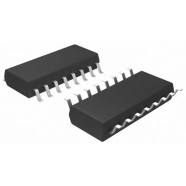
◆ Packaging type: SOP16


