CA51F652S6B
The CA51F652 series chip is a microcontroller based on the 1T 8051 core, which typically runs 10 times faster than traditional 8051 chips and has superior performance. The chip is equipped with 16KB Flash program memory, which can be repeatedly programmed, and 1280Byte SRAM, making it convenient for customers to develop rich applications. The chip has 26 built-in 12 bit ADCs, 26 touch buttons (no external capacitors required), and 6 16 bit PWM supports complementary and anti dead zone functions; It also has one I2C, two UART, SPI and other functional modules built-in. Supports PWM, I2C, UART peripherals that can be mapped to any pin, 9 high current pins, supports LED dot matrix scanning LED screen dual scanning display function, supports IDLE, STOP, and low-speed operation three power-saving modes to adapt to applications with different power consumption requirements. The powerful functionality and superior CS/EFT anti-interference performance make it widely applicable in household appliances and consumer products.

Product Details
kernel
CPU:1T 8051, 10 times faster than traditional 8051 with higher speed
Compatible with 8051 instruction set, dual DPTR working mode
memory
Flash: 16K bytes, supports multiple repeated erasures
15.5K program space, 512Byte data space available for storing power down data, saving EEPROM
RAM: 256 Byte internal RAM, 1024 Byte external RAM
Working Voltage
Working voltage: 2.0V~5.5V
Operating Temperature
Working temperature: -40 ℃~+105 ℃
clock system
External low-speed oscillator: 32.768KHz
Built in low-speed RC oscillator: 128KHz
Built in high-speed RC oscillator: 1MHz, accuracy of ± 1% @ 25 ℃ (factory calibrated)
PLL multiplier clock: 24MHz, accuracy of ± 1% 5V@25 ℃
timer
Three 16 bit universal timers: Timer 0, Timer 1, Timer 2
General Purpose Input/Output Port (GPIO)
Supports up to 26 GPIO ports,
Supports push-pull, open drain, pull-up, pull-down, and high impedance modes
IO current push 4 levels optional: 6mA, 10mA, 15mA, 20mA @ VDD=5V
Ordinary IO current level 2 optional: 18mA, 36mA @ VDD=5V
Support (LED0-LED8) 9 large current pins, with a higher capacity of up to 120mA@5V , can be used for high brightness LED screen display
TMC function
The clock source for TMC timer can be selected as IRCL or XOSCL
Minimum interruption time unit, 128 1/4 IRCL clock cycles or 128 XOSCL clock cycles
Configurable interrupt time ranges from 1-256 minimum unit times
Interrupt system
7 valid interrupt sources
Two level interrupt priority, supporting interrupt nesting
5 external interrupt sources INT0~INT4
External interrupt trigger edge selection: INT0~1 (rising edge, falling edge), INT2~4 (rising edge, falling edge, double edge)
Interrupt input pin selection: INT0 (P0.0), INT1 (P0.1), INT2 (P0.2), INT3 (P0.3), INT4 can choose any GPIO pin other than P0.0~P0.3 as the interrupt input pin
LED dot matrix (dual scan) control module
Built in LED dot matrix scanning module, supporting up to 8x9 pixels (LED0-LED8), LED driver with 8-level adjustable brightness
Analog to Digital Converter (ADC)
Supports 26 channels of 12 bit SAR ADC
Supports 3 types of reference voltage sources: VDD and internal reference, external reference
Selecting internal voltage as the reference, the internal channel can measure 1/4 VDD and can be used to measure the supply voltage
Touch Key
Built in touch sensing controller
Larger support for 26 touch channels, no need for external capacitors
High anti-interference performance, compliant with EMC (CS dynamic 10V, EFT 4KV) standards
Support touch interruption
Support low-power mode
16 bit PWM
Supports 6 PWM outputs, each can be individually controlled, and the cycle and duty cycle can be configured freely within the 16 bit range
Supports complementary mode and dead zone control, supports adjustable edge alignment and center alignment modes
Support direct output of internal clock function
Support PWM interrupt function
Each PWM output pin can be mapped to different GPIO pins
Universal Serial Interface (UART1/UART2)
Supports 2 full duplex serial ports
Support 1-byte receive cache
The TX/RX function of UART1/UART2 can be mapped to all other GPIO pins
I2C interface
Built in 1 I2C interface, supports master-slave mode, and supports standard/fast/high-speed modes
The SCL/SDA function of I2C pin can be mapped to all other GPIO pins
SPI interface
Built in 1 4-wire SPI interface, supporting master-slave mode
Low Voltage Detection (LVD)
The detection voltage can be set to 2.2V, 2.5V, 2.7V, 3.0V, 3.3V, 3.6V, 3.9V, and 4.2V.
Low voltage reset or interrupt can be set
Reset mode
The chip supports multiple reset sources: power on/off reset, soft reset, watchdog reset, low voltage detection reset
watchdog
27 bit watchdog timer, 16 bit adjustment accuracy, configurable watchdog reset or interrupt
Program download and simulation
Support ISP and IAP
Support online simulation function
low power consumption
STOP mode, current<7uA
IDLE mode, current<30uA
Low speed operation mode, current<12uA
Encapsulation type: SOP28

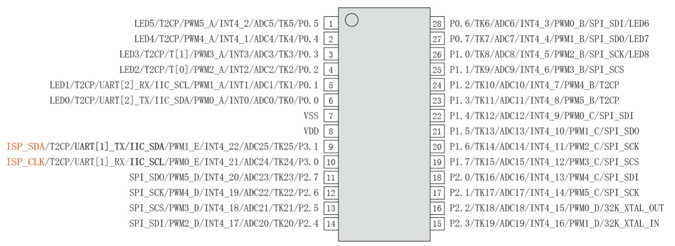
CA51F652S6B pin diagram


